


What is Xilinx ZCU102?
Introduction
The Zynq® UltraScale+™ MPSoC family is based on the Xilinx® UltraScale™ MPSoC architecture, integrating a feature-rich, 64-bit ARM-based quad- or dual-core processing system (PS) and Xilinx programmable logic (PL) UltraScale architecture in a single device. Also included are on-chip memory, multiport external memory interfaces, and rich peripheral interfaces, notably a 16.3 Gbps GTH transceiver that supports interfacing with PCI Express® Gen3 storage devices like NVMe SSD drives. This article will introduce the basics of the ZCU102 evaluation kit including an overview, specifications, user guide, features, and applications.
Table of Content
Xilinx ZCU102 Overview
Designed for rapid prototyping, the ZCU102 is a multipurpose evaluation board that utilizes the Zynq® UltraScale+TM XCZU9EG-2FFVB1156E MPSoC (multiprocessor system-on-chip). High-speed DDR4 SODIMM and component memory interfaces, FMC expansion ports, multi-gigabit per second serial transceivers, a variety of peripheral interfaces, and FPGA logic for user-customized designs provide a flexible prototyping platform.
The ZCU102 evaluation kit helps designers quickly start designing for automotive, industrial, video, and communications applications. Featuring Zynq™ UltraScale+™ MPSoC devices based on AMD's 16nm FinFET+ programmable logic architecture, the kit offers a quad-core ARM® Cortex®-A53, dual-core Cortex-R5F real-time processor and a Mali™-400 MP2 image processing unit. The ZCU102 allows for the development of numerous applications by supporting all key peripherals and interfaces.
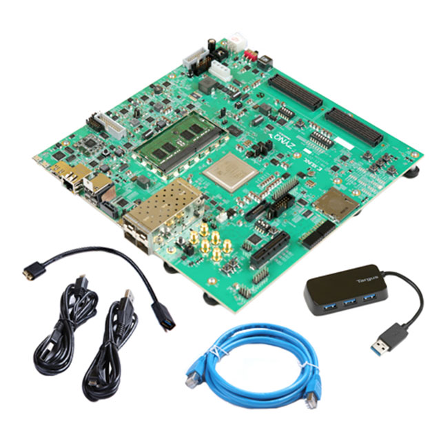
Figure1: ZCU102 evaluation kit
Xilinx ZCU 102 Features
- Optimized for quick application prototyping with Zynq Ultrascale+ MPSoC
- DDR4 SODIMM – 4GB 64-bit w/ ECC attached to Processor Subsystem (PS)
- DDR4 Component – 512MB 16-bit attached to Programmable Logic (PL)
- PCIe Root Port Gen2x4, USB3, Display Port & SATA
- 2x FPGA Mezzanine Card (FMC) interfaces for I/O expansion including 16 x 16.3 Gb/s GTH transceivers and 64 user-defined differential I/O signals
Xilinx ZCU102 block diagram
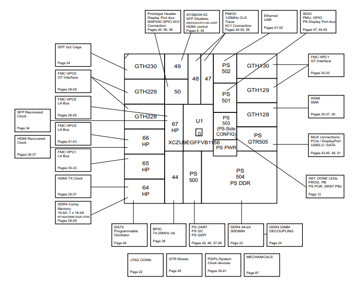
Figure: ZCU102 Evaluation Board Block Diagram
ZCU102 user guide
ZCU102 Board Characteristics
- XCZU9EG-2FFVB1156E MPSoC
- PL VCCINT for range in datasheet
- PCIe Gen2x4 Host form factor and Micro-ATX chassis footprint
- Configuration from QSPI
- Configuration from SD card
- Configuration over JTAG with PC4 header
- JTAG configuration using an Arm 20-pin header
- Configuration over USB-to-JTAG Bridge
- Clocks (PL-system, PS_CLK, Programmable Clock, SMA, SMA_GT_REF, Ethernet, USB)
- 64-bit SODIMM PS DDR4
- A 16-bit PL DDR4 component
- PS GTR assignment
°SATA
°DisplayPort
°USB3
°PCIe Gen2x4 Root Port
- PL GTH assignment
°PL GT assignments for FMC #1 (8 GTH) and FMC #2 (8 GTH)
°PL GT assignment for High-Definition Multimedia Interface (HDMITM) technology (3 GTH)
°SFP+ (4 GTH) PL GT assignment
°SMA (1 GTH) PL GT assignment
- PL FMC HPC #1 Connectivity - Full LA Bus
- PL FMC HPC #2 Connectivity - Partial LA Bus
- PS MIO: QSPI
- PS MIO: Ethernet
- PS MIO: USB2 (same connector as USB3)
- PS MIO: SD
- PS MIO: CAN
- PS MIO: UART (using USB-to-UART bridge)
- PS MIO: second UART
- PS MIO: I2C shared across PS and PL
- PS/PL EMIO: Trace
- PL-side UART
- PL-side LEDs (8)
- PL-side DIP switch (8-position)
- PL-side pushbuttons (5)
- PS-side pushbutton (1)
- PS-side LED (1)
- System user switches (PROG, CPU Reset)
- PJTAG
- Security - PSBATT button battery backup
- SYSMON
- Operational switches (Power on/off, PROG, Boot mode)
- Operational status LEDs (power supply status, INIT, DONE, PG, JTAG status, DDR power good)
- Power Management
ZCU102 Board Specifications
- Dimensions Width: 9.350 in. (23.749 cm)
- Length: 9.600 in. (24.384 cm)
- Thickness: 0.104 in. (0.2642 cm)
- Environmental Temperature Operating: 0°C to +45°C
- Storage: -25°C to +60°C
- Humidity:10% to 90% non-condensing
- Operating Voltage:+12 VDC
ZCU102 Application
- Automotive
- Industrial
- Video
- Communications
ZCU102 manufacturer
The top supplier of comprehensive programmable logic solutions worldwide is Xilinx. A vast array of cutting-edge integrated circuits, software development tools, and IP (intellectual property) cores with preset system-level functionalities are developed, produced, and marketed by Xilinx. Customers program devices to carry out particular logic processes using automation software tools and intellectual property (IP) from Xilinx and its partners. In 1984, Xilinx was established. In 1985, Xilinx introduced its first commercial product, the field programmable logic array (FPGA), which was a revolutionary technological advancement. Presently, about half of the global demand for FPGA products is satisfied by Xilinx. Additionally, complex programmable logic devices (CPLDs) are part of the Xilinx product line. In certain control applications, CPLDs typically outperform FPGAs in terms of speed, although they offer fewer logic resources.
 A Comprehensive Guide to Grasping FPGA Structure6/20/2024 664
FPGA (Field-Programmable Gate Array) is an integrated circuit, a type of programmable chip, that allows engineers to program custom digital logic. It can change its hardware logic based on the program, with the primary purpose of enabling engineers to redesign and reconfigure their chips faster and cheaper, whenever they want. However, nothing in the world is ideal, and FPGA chips also have limitations!
Read More > The EU to Impose Tariffs on Electric Vehicle Imports from China in Early July6/17/2024 336
The EU to Impose Tariffs on Electric Vehicle Imports from China in Early July
Read More > What is XC7A100T-2FG484I?6/6/2024 496
XC7A100T-1CSG324C is an FPGA-based digital signal processing board, which consists of Xilinx's Virtex-7 series chips and FPGA interface chips.
Read More > Analog cycle inventory hits bottom, AI drives flash memory demand to continue6/4/2024 496
Analog cycle inventory hits bottom, AI drives flash memory demand to continue
Read More > Micron Plans to Build a Factory in Japan, NAND Flash Prices May Remain High5/31/2024 726
Micron Plans to Build a Factory in Japan, NAND Flash Prices May Remain High
Read More >
Hot News
- Diode Overview: Application in Automotive Alternator Rectifiers
- Electronic Component Symbols: Resistor, Capacitor, Transformers and Connectors
- Voltage-Controlled Oscillator: Principle, Type Selection, and Application
- Ultra-low power consumption of STM32U575/585 microcontrollers(MCU)
- What is Xilinx 7 Series FPGA Clock Structure- -Part two
- Basic Information about Temperature Sensor
SUPPORT
ABOUT BITFOIC
QUICK LINKS
Connect with us
Tel: 86-755-23606554
E-mail: [email protected]
Address: Room A29, 24 / F, Hoi Tak Wai, Prince Edward industrial building, 706 Prince Edward Road East, San Po Kong, Kowloon,Hongkong
Mon-Fri: 09.30 AM - 18.30 PM


