


Zedboard zynq-7000: Zynq 7000 datasheet, Features, Architecture and Core Components
Introduction
The ZedBoard Zynq-7000 is a cutting-edge embedded computing platform that seamlessly merges a dual-core ARM Cortex-A9 CPU and Xilinx's programmable logic, making it a versatile option for a wide range of applications. This article introduces the Zynq-7000 platform using the ZedBoard development board launched by Avnet. Simultaneously, we will explore ZedBoard and Zynq-7000 Architecture and Core Components.
Table of Content
What is Zynq?
Zynq is an APSoC, which integrates computer components into a single chip and includes FPGA technology. FPGAs are typically employed as independent components to prototype custom system chips or to create hardware that will eventually be converted into application-specific integrated circuits (ASICs). As a result, the "system" in APSoC about Zynq refers to the combination of twin dedicated processors (twin-core ARM Cortex-A9 Processors) and FPGA technology. Developers can take advantage of both processor and FPGA functions.
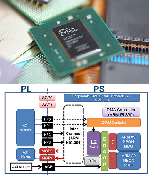
Figure1-Zynq
What is Zedboard?
Digilent's ZedBoard offers an affordable development platform tailored for the Xilinx Zynq-7000 all-programmable SoC (AP SoC). It encompasses all essential components for constructing designs based on Linux, Android, Windows, or alternative OS/RTOS. Furthermore, user-friendly access is facilitated through various expansion connectors that unveil both the processing system and programmable logic I/Os.
ZedBoard seamlessly integrates with the SDSoC™ environment. The SDSoC development platform delivers a recognizable development experience for embedded C/C++ applications, featuring a user-friendly Eclipse IDE and an extensive design environment tailored for the heterogeneous Zynq AP SoC.
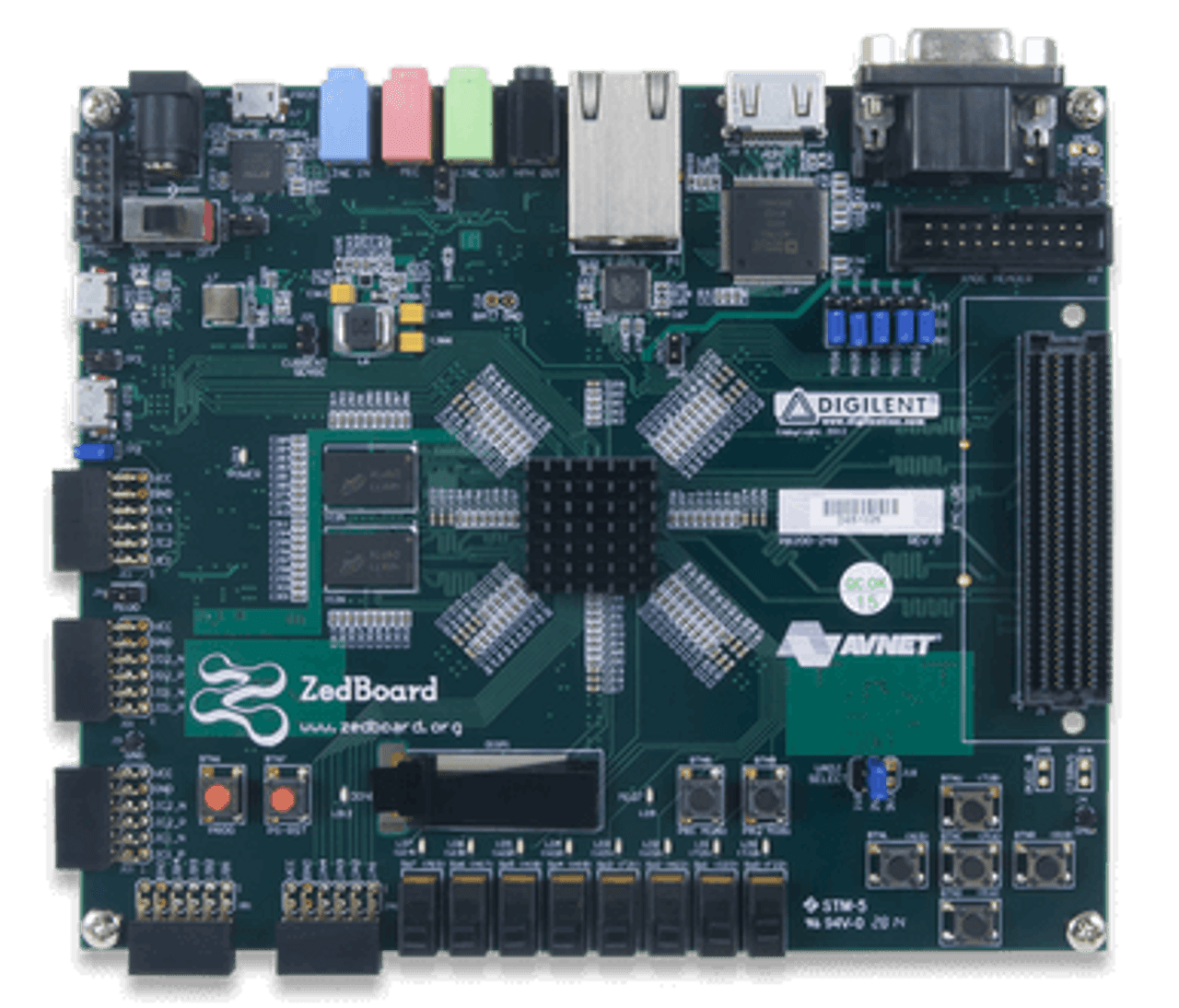
Figure2-Zedboard
ZedBoard Zynq-7000 Architecture and Core Components
The ZedBoard Zynq-7000 is powered by the Xilinx Zynq-7000 All Programmable System-on-Chip (SoC). This breakthrough technology combines a dual-core ARM Cortex-A9 processor with programmable logic, resulting in a unique combination of computing power and flexibility. The Cortex-A9 cores provide high-performance processing capabilities, and the programmable logic enables hardware customization to satisfy unique application needs.
Zedboard Zynq-7000 Overview
The ZedBoard development board is based on the Xilinx Zynq-7000 All Programmable Soc and integrates the PS processing unit and PL logic unit of the dual-core Cortex-A9. On Zynq, the ARM Cortex-A9 is an application-level processor capable of running complete operating systems like Linux, while the editable logic PL is based on the Xilinx 7 series FPGA architecture. This framework implements the industry standard AXI interface link, achieving a high-bandwidth, low-latency link between the two parts of the chip. This means that overhead can be reduced while allowing each part to perform optimally. The SOC is integrated into one, reducing physical overhead and overall R&D costs.
Zynq-7000 Architecture and Core Components
The Zynq-7000 is built around Xilinx's FPGA technology, which allows for programmable logic and the customization of hardware designs. This capability enables developers to create bespoke hardware accelerators, interfaces, and peripherals to meet the specific requirements of various applications. The Zynq-7000 architecture also features on-chip memory resources, including L1 and L2 caches for the ARM cores, ensuring efficient data access.
Zynq-7000 Basic Architecture
The Zynq7000 architecture is divided into the PS side and the PL side. These two parts divide the IO BANK of Zynq7000 into different modules. The specific BANK resource division is shown in Figure3
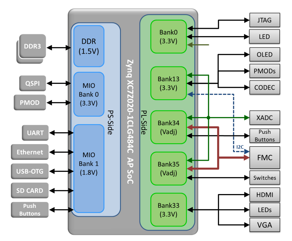
Figure3-Zynq-7000 Basic Architecture
Zedboard basic framework
The ZedBoard development board launched by Avnet customizes peripherals based on the resources of Zynq7000 and makes full use of the resource advantages of PS and PL for early project technical evaluation. The ZedBoard development board uses the resource peripheral principle block of Zynq7000 as shown in Figure 4.
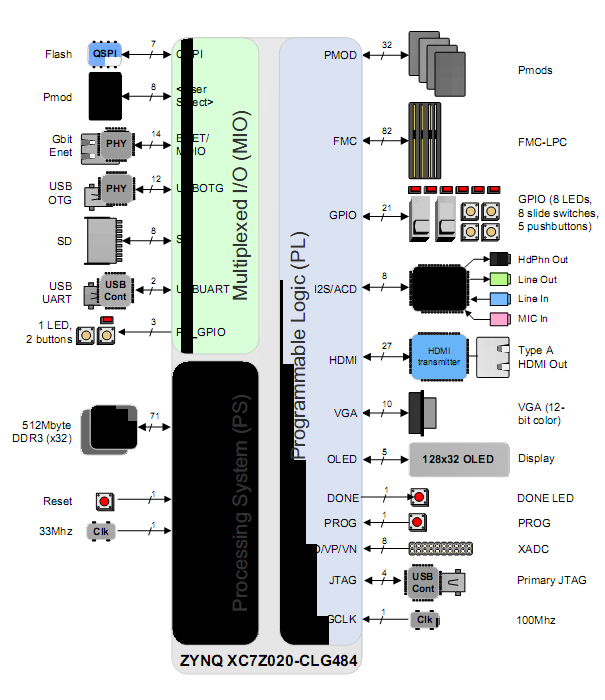
Figure4-Zedboard basic framework
The actual ZedBoard development board is shown in Figure 5. JP marks the location of the jumper cap.
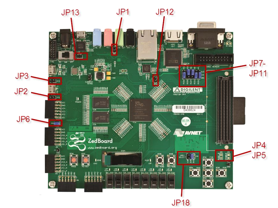
Figure5-ZedBoard development board JP
Zedboard Zynq-7000 SoC Product Features
- Xilinx Zynq-7000 AP SoC XC7Z020-CLG484
- Dual-core Arm Cortex®-A9
- 512 MB DDR3
- 256 MB quad-SPI Flash
- 4 GB SD card
- On-board USB-JTAG programming
- 10/100/1000 Ethernet
- USB OTG 2.0 and USB-UART
- Analog devices ADAU1761 SigmaDSP® stereo, low-power, 96 kHz, 24-bit Audio Codec
- Analog devices ADV7511 high-performance 225 MHz HDMI transmitter (1080p HDMI, 8-bit VGA, 128 x 32 OLED)
- PS and PL I/O expansion (FMC, Pmod, and XADC)
Zedboard Zynq-7000 Applications
- Video processing
- Reconfigurable computing
- Motor controls
- Software acceleration
- Embedded Linux
- RTOS development
Zedboard Zynq-7000 Schematic
Zedboard Zynq-7000 Schematic Datasheet
Figure5-Zedboard Zynq-7000 Schematic Datasheet
Zedboard Zynq-7000 Datasheet
 A Comprehensive Guide to Grasping FPGA Structure6/20/2024 678
FPGA (Field-Programmable Gate Array) is an integrated circuit, a type of programmable chip, that allows engineers to program custom digital logic. It can change its hardware logic based on the program, with the primary purpose of enabling engineers to redesign and reconfigure their chips faster and cheaper, whenever they want. However, nothing in the world is ideal, and FPGA chips also have limitations!
Read More > The EU to Impose Tariffs on Electric Vehicle Imports from China in Early July6/17/2024 342
The EU to Impose Tariffs on Electric Vehicle Imports from China in Early July
Read More >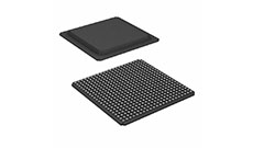 What is XC7A100T-2FG484I?6/6/2024 502
XC7A100T-1CSG324C is an FPGA-based digital signal processing board, which consists of Xilinx's Virtex-7 series chips and FPGA interface chips.
Read More > Analog cycle inventory hits bottom, AI drives flash memory demand to continue6/4/2024 510
Analog cycle inventory hits bottom, AI drives flash memory demand to continue
Read More > Micron Plans to Build a Factory in Japan, NAND Flash Prices May Remain High5/31/2024 733
Micron Plans to Build a Factory in Japan, NAND Flash Prices May Remain High
Read More >
Hot News
- Diode Overview: Application in Automotive Alternator Rectifiers
- Electronic Component Symbols: Resistor, Capacitor, Transformers and Connectors
- Voltage-Controlled Oscillator: Principle, Type Selection, and Application
- Ultra-low power consumption of STM32U575/585 microcontrollers(MCU)
- What is Xilinx 7 Series FPGA Clock Structure- -Part two
- Basic Information about Temperature Sensor
SUPPORT
ABOUT BITFOIC
QUICK LINKS
Connect with us
Tel: 86-755-23606554
E-mail: [email protected]
Address: Room A29, 24 / F, Hoi Tak Wai, Prince Edward industrial building, 706 Prince Edward Road East, San Po Kong, Kowloon,Hongkong
Mon-Fri: 09.30 AM - 18.30 PM


