


AT89S52 CMOS 8-bit microcontroller: Pinout, Datasheet, CAD Model and Features
The AT89S52 is less power-consuming, highly reliable, has the ability to get data up to eight-bit, and is constructed with the CMOS (Complementary metal-oxide-semiconductor) technique. This post will share the AT89S52 pinout, datasheet, CAD Model, Features, and application.
ⅠAT89S52 Description
The AT89S52 is a low-power, high-performance CMOS 8-bit microcontroller with 8K bytes of in-system programmable Flash memory. The device is manufactured using Atmel’s high-density nonvolatile memory technology and is compatible with the industry-standard 80C51 instruction set and pinout. The on-chip Flash allows the program memory to be reprogrammed in-system or by a conventional nonvolatile memory programmer. Combining a versatile 8-bit CPU with in-system programmable Flash on a monolithic chip, the Atmel AT89S52 is a powerful microcontroller that provides a highly-flexible and cost-effective solution to many embedded control applications.
AT89S52 integrates a general-purpose 8-bit CPU, memory (including RAM and Flash ROM), parallel IO interface, timer/counter, interrupt control functions, etc. on one chip, and the functional modules in the chip are connected to each other through the internal bus. AT89S52 has three package structures, and the pin arrangement of the PDIP package is shown in Figure 4.1. The main functional modules of the AT89S52 microcontroller are introduced as follows.
ⅡCAD Model
Symbol

Figure1-1 Symbol
Footprint
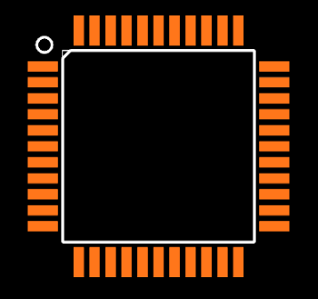
Figure1-2 footprint
CAD Model

Figure1-3 CAD Model
ⅢAT89S52 Pinout
40-lead PDIP

Figure1-40-lead PDIP
44-lead PLCC
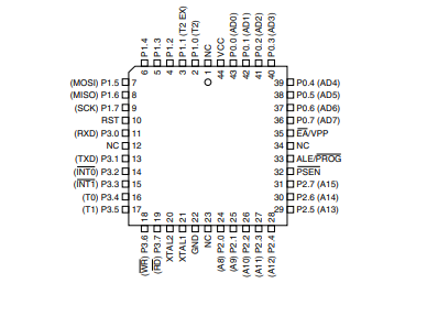
Figure2-44-lead PLCC
lead TQFP

Figure3-44-lead TQFP
ⅣAT89S52 Pin Configuration
|
Pin Number |
Pin Name |
Description |
|
1 |
P1.0 (T2) |
Timer/Counter or 0th GPIO pin of PORT 1 |
|
2 |
P1.1 (T2.EX) |
Timer/Counter/External Counter or 1st GPIO pin of PORT 1 |
|
3 |
P1.2 |
2nd GPIO pin of PORT 1 |
|
4 |
P1.3 |
3rd GPIO pin of PORT 1 |
|
5 |
P1.4 |
4th GPIO pin of PORT 1 |
|
6 |
P1.5 (MOSI) |
MOSI for System Programming or 5th GPIO pin of PORT 1 |
|
7 |
P1.6 (MISO) |
MISO for System Programming or 6th GPIO pin of PORT 1 |
|
8 |
P1.7 (SCK) |
SCK for System Programming or 7th GPIO pin of PORT 1 |
|
9 |
RST |
Making this pin high will reset the Microcontroller |
|
10 |
P3.0 (RXD) |
RXD Serial Input or 0th GPIO pin of PORT 3 |
|
11 |
P3.1 (TXD) |
TXD Serial Output or 1st GPIO pin of PORT 3 |
|
12 |
P3.2 (INT0’) |
External Interrupt 0 or 2nd GPIO pin of PORT 3 |
|
13 |
P3.3 (INT1’) |
External Interrupt 1 or 3rd GPIO pin of PORT 3 |
|
14 |
P3.4 (T0) |
Timer 0 or 4th GPIO pin of PORT 3 |
|
15 |
P3.5 (T1) |
Timer 1 or 5th GPIO pin of PORT 3 |
|
16 |
P3.6 (WR’) |
Memory Write or 6th GPIO pin of PORT 3 |
|
17 |
P3.7 (RD’) |
Memory Read or 7th GPIO pin of PORT 3 |
|
18 |
XTAL2 |
External Oscillator Output |
|
19 |
XTAL1 |
External Oscillator Input |
|
20 |
GND |
Ground pin of MCU |
|
21 |
P2.0(A8) |
0th GPIO pin of PORT 2 |
|
22 |
P2.1 (A9) |
1st GPIO pin of PORT 2 |
|
23 |
P2.2 (A10) |
2nd GPIO pin of PORT 2 |
|
24 |
P2.3 (A11) |
3rd GPIO pin of PORT 2 |
|
25 |
P2.4 (A12) |
4th GPIO pin of PORT 2 |
|
26 |
P2.5 (A13) |
5th GPIO pin of PORT 2 |
|
27 |
P2.6 (A14) |
6th GPIO pin of PORT 2 |
|
28 |
P2.7 (A15) |
7th GPIO pin of PORT 2 |
|
29 |
PSEN’ |
Program store Enable used to read external program memory |
|
30 |
ALE / PROG’ |
Address Latch Enable / Program Pulse Input |
|
31 |
EA’ / VPP |
External Access Enable / Programming enables Voltage |
|
32 |
P0.7 (AD7) |
Address / Data pin 7 or 7th GPIO pin of PORT 0 |
|
33 |
P0.6 (AD6) |
Address / Data pin 6 or 6th GPIO pin of PORT 0 |
|
34 |
P0.5 (AD5) |
Address / Data pin 5 or 5th GPIO pin of PORT 0 |
|
35 |
P0.4 (AD4) |
Address / Data pin 4 or 4th GPIO pin of PORT 0 |
|
36 |
P0.3 (AD3) |
Address / Data pin 3 or 3rd GPIO pin of PORT 0 |
|
37 |
P0.2 (AD2) |
Address / Data pin 2 or 2nd GPIO pin of PORT 0 |
|
38 |
P0.1 (AD1) |
Address / Data pin 1 or 1st GPIO pin of PORT 0 |
|
39 |
P0.0 (AD0) |
Address / Data pin 0 or 0th GPIO pin of PORT 0 |
|
40 |
VCC |
Positive pin of MCU (+5V) |
ⅤAT89S52 Microcontroller Features
|
CPU |
8-bit PIC |
|
Number of Pins |
40 |
|
Operating Voltage (V) |
4 to 5.5 V |
|
Number of Programmable I/O pins |
32 |
|
ADC Module |
Nil |
|
Timer Module |
16-bit(1) |
|
Comparators |
Nil |
|
DAC Module |
Nil |
|
Communication Peripherals |
UART(1) |
|
External Oscillator |
Up to 23Mhz |
|
Internal Oscillator |
Nil |
|
Program Memory Type |
Flash |
|
Program Memory (KB) |
8KB |
|
CPU Speed (MIPS) |
- |
|
RAM Bytes |
256 x 8-bit |
|
Data EEPROM |
Nil |
ⅥAT89S52 Specifications
|
Features and Peripherals |
Availability |
|
Architecture |
8-bit PIC |
|
Pin Count |
40 |
|
RAM |
256 Bytes |
|
EEPROM/HEF |
No |
|
Program Memory |
8 KiloBytes |
|
CPU speed |
33 MHz |
|
Internal Oscillator |
No |
|
Number of Comparators |
2 |
|
ADC |
No |
|
DAC |
No |
|
Number of Programmable I/O pins |
32 |
|
Window Watchdog Timer |
No |
|
External Oscillator Frequency |
23 MHz (max) |
|
Resolution of PWM |
No |
|
Number of 16-bit Timers |
3 |
|
Program Memory Type |
Flash |
|
UART module |
1 |
|
Power-off Flag |
Yes |
|
Dual Data Pointer |
Yes |
|
Operating Voltage |
4V – 5.5 V |
|
Operating Temperature |
-550C – 1250C |
ⅦAT89S52 Features
- Compatible with MCS®-51 Products
- 8K Bytes of In-System Programmable (ISP) Flash Memory – Endurance: 10,000 Write/Erase Cycles
- 4.0V to 5.5V Operating Range
- Fully Static Operation: 0 Hz to 33 MHz
- Three-level Program Memory Lock
- 256 x 8-bit Internal RAM
- 32 Programmable I/O Lines
- Three 16-bit Timer/Counters
- Eight Interrupt Sources
- Full Duplex UART Serial Channel
- Low-power Idle and Power-down Modes
- Interrupt Recovery from Power-down Mode
- Watchdog Timer
- Dual Data Pointer
- Power-off Flag
- Fast Programming Time
- Flexible ISP Programming (Byte and Page Mode)
- Green (Pb/Halide-free) Packaging Option
ⅧAT89S52 Block Diagram
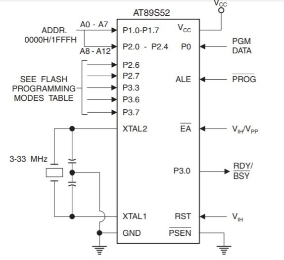
Figure4-40-lead PDIP
ⅨHow to Select your Atmel Microcontroller
Microchip provides a wide variety of Microcontrollers from the PIC family and the Atmel Family. Their collection has just piled up after Microchip acquired Atmel. Each MCU has its own advantage and disadvantage. There are many parameters that one has to consider before selecting an MCU for his/her project. The below points are suggestions that might help one select an MCU.
- If you are a beginner learning Microcontroller, selecting an MCU with good online community support and wide applications will be a good choice. For Atmel AT89S52 or ATmega328 will be a good choice.
- Consider the operating voltage of your system. If they are 5V then select a 5V MCU some sensors or devices work and communicate on 3.3V in such case a 3.3V MCU can be selected
- If size and price are limitations then you can choose small 8-pin MCUs like Attiny1614. These are also comparatively cheaper.
- Based on the sensors and actuators used in your project, verify which modules you might need for MCU. For example, is you are reading many Analog voltages then make sure MCU has enough ADC channels and supportive resolution. The details of all modules are given in the table above.
- If your project involves communication protocols like UART, SPI, I2C, CAN, etc make sure your MCU can support them. Some MCU can support more than one module of the same protocol
ⅩApplications
- Multiple DIY Projects
- Excellent choice if you are learning ATmel
- Projects requiring Multiple I/O interfaces and communications
- Replacement for Arduino Module
- Ideal for more advanced level A/D applications in automotive, industrial, appliances, and consumer applications.
Ⅺ AT89S52 Package PSDIP

Figure5-package
Ⅻ How to program AT89S52 8-bit Microcontroller
Different software and compilers available in the market can be used to program the Atmel microcontrollers family.
Support Compilers
Components Needed
- IDE
- IPE
- a suitable compiler
- a programmer/debugger to develop a program
A programming environment is what an IDE (Integrated Development Environment) is there to deliver. The software is transformed into readable HEX files by the compiler. HEX files are burned in AVR MCUs using the IPE (Integrated Programming Environment). We frequently use Keil uVision IDE for IDE.
USBASP is an In-circuit programmer/debugger which plays an integral role in programming microcontrollers. It supports In-Circuit-Serial-Programming and is operated by a computer to burn the code into AT89S52 8-bit microcontroller. For hardware programming, it is purchased separately. It is advised to simulate the program beforehand on the software for optimization and error-free programs. Furthermore, hardware like a 12 Volts adapter, 7805 Voltage Regulator, Crystal Oscillator, and capacitors are required.
The picture below is the connection diagram for programming the AT89S52 controller:
Figure4- connection diagram
XIII AT89S51 vs AT89S52
AT89S51:
- 8051-based Full Static CMOS controller with Three-Level Program Memory Lock, 32 I/O lines, 2 Timers/Counters, 6 Interrupts Sources, Watchdog Timer, 2 DPTRs 4K Flash, 128 Bytes On-chip RAM.
AT89S52:
- 8051-based Full Static CMOS controller with Three-Level Program Memory Lock, 32 I/O lines, 3 Timers/Counters, 8 Interrupts Sources, Watchdog Timer, 2 DPTRs, 8K Flash Memory, 256 Bytes On-chip RAM.
- In AT89S52, user RAM is from 00H to FFH. In this lower 128 bytes are both directly and indirectly addressed. The upper 128 bytes are only indirectly addressed.
In AT89S52, all the ports are dual-functionality whereas in AT89S51, only three ports are.
XIV AT89S52 PDF
AT89S52 Datasheet
 DC-DC converter RFB-0505S: Specification,Datasheet,Features and Applications6/13/2024 425
The RFB-0505S is a DC-DC converter from RECOM Power, Inc., belonging to the RFB Series. It features a Single In-Line Package (SIP7) and provides a single unregulated output. This converter offers 1 watt of power with an output voltage of 5V and is rated for an isolation voltage of 1kV.
Read More >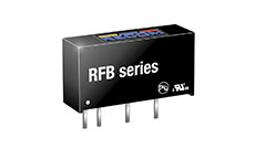 Understanding the RFMM-0505S DC-DC Converter: A Comprehensive Guide6/4/2024 601
In the world of electronics, ensuring efficient power management is crucial for the performance and reliability of devices. One of the key components in achieving this is the DC-DC converter. Today, we dive into the specifics of the RFMM-0505S DC-DC converter, exploring its features, applications, and benefits.
Read More >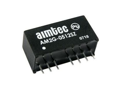 12V DC-DC Converter AM2G-0512SZ: Specifications, Datasheet, Applications and Features6/3/2024 512
A DC-DC converter is an essential electronic device to convert a direct current (DC) source from one voltage level to another. These converters are widely employed in various applications, including portable electronic devices, automotive systems, and renewable energy installations.
Read More >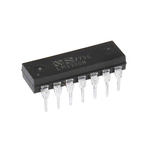 What is LM3900 Quadruple Norton Operational Amplifier?5/30/2024 1093
The LM3900 consists of four independent dual-input internally compensated amplifiers. These amplifiers are specifically designed to operate on a single power supply voltage and provide a large output voltage swing. They utilize current mirrors to achieve in-phase input functionality. Applications include AC amplifiers, RC active filters, low-frequency triangle waves, square wave, and pulse waveform generation circuits, tachometers, and low-speed, high-voltage digital logic gates.
Read More >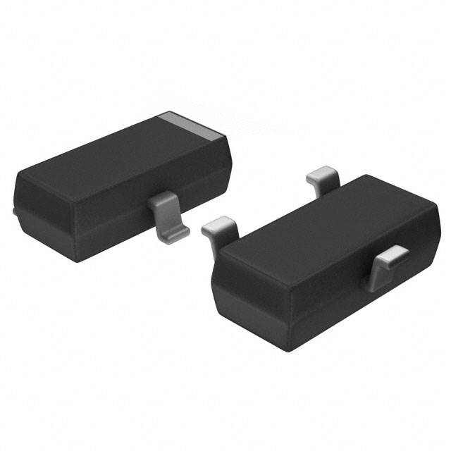 Exploring the MMBT3906 Transistor: A Comprehensive Guide5/24/2024 730
The goal of the Taiwan Semiconductor MMBT3906 PNP Bipolar Transistor is to provide a high surge current capability with minimal power loss. This transistor is perfect for automated installation and has high efficiency.
Read More >
SUPPORT
ABOUT BITFOIC
QUICK LINKS
Connect with us
Tel: 86-755-23606554
E-mail: [email protected]
Address: Room A29, 24 / F, Hoi Tak Wai, Prince Edward industrial building, 706 Prince Edward Road East, San Po Kong, Kowloon,Hongkong
Mon-Fri: 09.30 AM - 18.30 PM


