


How to use and test TL431 Shunt Regulator? (with circuit examples)
Introduction
Do you require power supply circuits for your project involving a linear regulator or an open-loop configuration? Or are you trying to find a device that can compare all voltage types? The TL431 circuits are the ideal solution in that case. Additionally, they are perfect for programmable shunt voltage reference or routine bandgap voltage reference operations. Despite being somewhat difficult to set up, the TL431 circuit is essential for voltage control and power supply control chips. Additionally, it has a temperature-corrected bandgap voltage reference.
Catalog
Ⅰ What is TL431 Shunt Regulator?
TL431 is a 2.50~36V adjustable precision shunt regulator produced by Texas Instruments (TI) and Motorola. It is a reference voltage source with adjustable current output capability. The TL431 is a three-terminal adjustable shunt regulator that offers good temperature stability. The typical dynamic output impedance is 0.2Ω, the adjustment range of the cathode current is 1-100mA, and the adjustable voltage value of 2.5V-36V can be realized. It can be used as a shunt voltage regulator, a series voltage regulator, a switch adjustment control circuit, a reference voltage, etc., and is widely used.
TL431 series products include TL431C, TL431AC, TL431I, TL431AI, TL431M, TL431Y, a total of 6 models. Their internal circuits are the same, only individual technical indicators are slightly different.
Ⅱ TL431 Pinout and Internal Structure
Pin Configuration
The TL431 regulator is a 3-terminal shunt regulator with certain thermal stability over applicable temperature ranges of automotive, military, and commercial. The TL431 regulator pin configuration/pin diagram is shown in the figure below.

Figure1- pin configuration
TL431 Internal Circuit Diagram
It consists of a multi-pole amplifier circuit, bias circuit, compensation, and protection circuit, among which transistor V1 constitutes the input pole, V3, V4, and V5 constitute the voltage regulation reference, V7, and V8 constitute the mirror constant current source, and V6, V9 constitute the differential amplifier As an intermediate stage, V10 and V11 form a composite tube to form an output, and other resistors, capacitors, and diodes play the role of bias, compensation, and protection respectively. In principle, it is a single-ended input and single-ended output DC amplifier.
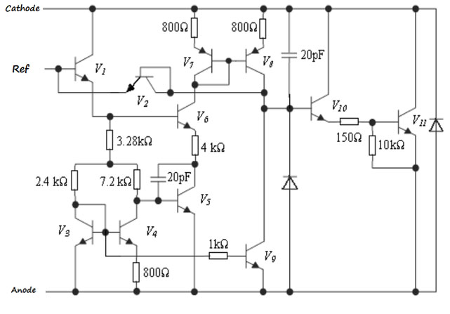
Figure2-Internal Circuit Diagram
Its equivalent functional diagram is shown in Figure 3. It consists of a 2.5V precision reference voltage source, a voltage comparator, and an output switch tube. The output voltage of the reference terminal is compared with the precision reference voltage source Vref. When the reference terminal voltage When exceeding 2.5V, TL431 conducts immediately.

Figure3-equivalent functional diagram
Ⅲ TL431 FEATURES
- Programmable Output Voltage to 40V
- Guaranteed 0.5% Reference Voltage Tolerance
- Low (0.2Ω Typ.) Dynamic Output Impedance
- Cathode Current Range(Continuous) – 100 ~ 150 mA
- Equivalent Full Range Temperature Coefficient of
- 50PPM/°C
- Temperature Compensated For Operation Over
- Full Rated Operating Temperature Range
- Low Output Noise Voltage
- Fast Turn-on Response
- TO-92, SOT-89 or SOT-23 3L Package
Ⅳ How to test TL431?
As shown in the figure below is the circuit tested with TL431, the power supply is 0~20V maintenance power supply.
An ammeter is connected between the cathode and the power supply, to observe the change of the cathode current with the change of the G electrode voltage. Then connect a voltmeter between the cathode and the anode, so that you can observe the change of the TL431 output with the power supply.
Before the test, adjust the potentiometer to near the middle value, then use a digital meter to measure the voltage of K pole to ground, and adjust the voltage output of the maintenance power supply. At this time, it can be found that the voltage between the cathode and the ground has only two states: one is about 2V (low level); the other is about 2V (low level). The other is equal to the supply voltage (high level).
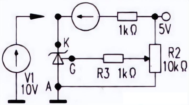
Figure4-how to test TL431
Ⅴ How to judge the quality of TL431?
For the online TL431 power supply error comparator, an external maintenance power supply can be used for detection. Connect the maintenance power supply to the sampling point of TL431. When the voltage is higher than the nominal voltage, TL431 is turned on and the cathode voltage is low.
That is to say, when the power supply voltage rises, the TL431 is turned on, so that the diode of the photocoupler is turned on, so that the triode is in a saturated state, and finally shortens the conduction time of the primary power switch (reduces the duty cycle). Thus, the output voltage is lowered.
If the maintenance voltage decreases, the TL431 will be cut off, the K pole voltage will be high, the diode of the photocoupler will be cut off, and the triode will be in the cut-off state, and the final control will increase the turn-on time of the primary power switch of the transformer (increase the duty cycle).
Increase the output voltage. The closed-loop voltage regulator circuit of the switching power supply uses the on or off state of TL431 to adjust the duty cycle of the switch to control the stability of the output voltage.
When measuring with a multimeter, if the resistance between the two poles of lC is normal, it can be judged that TL431 is normal. When using the maintenance power supply for the power-on test, when the power supply voltage is changed, if the TL431 pole-to-ground level changes twice, it can be judged that the TL431 is normal.
Ⅵ How do TL431 circuits work? (3 testing circuit examples)
6.1 Threshold output voltage test
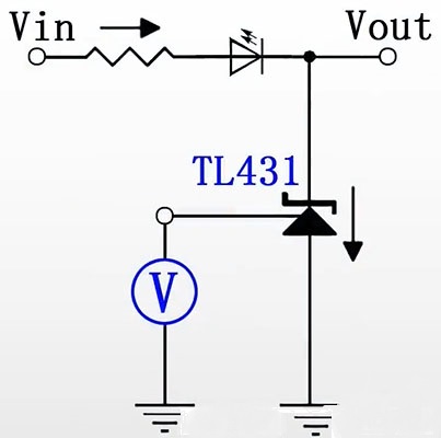
Figure5-Voltage test circuit diagram
Connect an adjustable voltage source to the reference terminal of TL431, connect a current limiting resistor and LED light between the power input terminal and K terminal, and connect a multimeter at the output terminal to detect the output voltage VKA.
The test results show that when the R terminal voltage source voltage is lower than 2.5V, the LED light is off, and the output voltage VKA is relatively large, about 17.36V, indicating that when VREF<2.5V, TL431 is cut off; when the R terminal voltage source When the voltage is higher than 2.5V, the LED light is on, and the output voltage VKA is small, about 1.9V, which means that when VREF>2.5V, the TL431 is turned on, the voltage of the K terminal is pulled down, and the LED light turns on and emits light. And as VREF (2.5-2.7V) increases, VKA decreases, but the decrease is not obvious (1.945-1.8V change), indicating that when VREF increases, the base current IB of the triode in Figure 5(a) increases Larger, the collector current IC increases a little bit, so that the divided voltage on the current limiting resistor also increases a little bit, then the voltage of VKA is pulled down a little bit, and the triode is in a saturated or critical saturated state.
6.2. 2.5V regulator circuit test

Figure6-2.5V regulator circuit test chart
Test circuit
As shown in Figure 7, an adjustable voltage source Vin is connected to the input terminal, and the current limiting resistor R is 2.7K. Connect the K terminal and the R terminal of the TL431, and test VKA with a digital multimeter at the output terminal.
Note: Since 431 only can pull down the voltage, it cannot boost the voltage. To achieve voltage regulation, the voltage source Vin must be >2.5V, where the initial value of Vin is 20V.
Circuit analysis
At first, when VKA>2.5V, 431 is turned on, K terminal and A terminal are short-circuited, and the voltage of K terminal is pulled down to VKA<2.5V, then 431 is immediately cut off, K terminal and A terminal are disconnected, and the voltage of K terminal rises again. When it reaches >2.5V, 431 is turned on again, and the cycle repeats. Since the turn-on and cut-off is a relatively fast processes, VKA finally stabilizes at 2.5V.
Test results
When Vin is 20V, the output voltage VKA=2.51V, if Vin is lowered or increased, VKA remains unchanged, and the voltage stabilization effect is achieved.
Note: The size of Vin needs to make IKA between 1-100mA, that is, 1mA<(Vin-2.5)/R<100mA, make sure to adjust Vin to make 5.7V<Vin<272.5V.
6.3 Adjustable voltage regulator circuit test
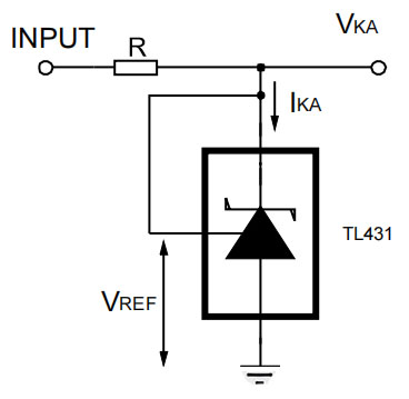
Figure7-Adjustable voltage regulator circuit test chart
(1) Test circuit
As shown in Figure 7, an adjustable voltage source Vin (initial setting is 20V) is connected to the input terminal, the current limiting resistor R is 2.7K, R1 is a 10K resistor, R2 is a 10K adjustable rheostat, and a digital multimeter is connected to the output terminal Test the VKA.
(2) Circuit analysis
After power-on, before TL431 is turned on, IREF=0, according to the principle of series voltage division, VREF=VIN/(R+R1+R2)*R2=8.81V, then VREF>2.5V, TL431 is turned on, then VKA is pulled low. After VKA is pulled down, the divided voltage on R1 and R2 decreases, and VREF decreases. When VREF drops to <2.5V, TL431 is cut off, the VKA voltage rises, the divided voltage on R1 and R2 increases, and the VREF voltage rises again. When the VREF voltage rises to >2.5V, TL431 has turned on again, VKA is pulled down again, and so on. Therefore, the voltage of the reference terminal is always dynamically regulated at 2.5V.
So how to analyze the voltage at the output terminal VKA?
According to the previous functional block diagram, the reference terminal R of 431 is connected to the non-inverting input terminal of the op-amp. Ideally, when the input impedance of the op-amp is above megohm, it can be considered that the input terminal of the op-amp has no current according to the principle of "virtual break". , ie IREF=0, and VREF=2.5V, so

Figure8-output terminal VKA
According to the manual, the maximum Iref is 4uA, and the actual VKA has an additional voltage of Iref*R1, mV level (4uA*10KΩ=40mV).

Figure9-VKA
(3) Test Results
When R1=10K, R2=10K, the output voltage VKA=5.094V, adjust the value of the power supply voltage Vin, and the output voltage value remains unchanged, always 5.094V.
Adjust R2, reduce the resistance of R2, VKA increases, and adjust the value of the power supply voltage Vin, the output voltage value remains unchanged, in line with the above analysis.
Summary
Based on the above three test circuits, the working principle of TL431 is analyzed. TL431 can realize switch control and 2.5V-36V regulated output. Experimenters can test it by themselves. In fact, in actual use, the working principle of the 431 series reference voltage regulator is the same, such as LTL431, which can be used as a substitute for TL431.
Ⅶ TL431 common application circuits
This is the circuit most used by 431, the output voltage Vout=(1+R1/R2)Vref. Any voltage output from 2.5V to 36V can be obtained by choosing different values of R1 and R2, especially, when R1=R2, VO=5V. Since the reference electrode input uses an emitter follower, it has a high input impedance and a small input current.
For this circuit, the basic analysis steps are:
1) Determine the regulated voltage
2) Determine the maximum load current
3) Confirm the working current of TL431 (1mA~100mA) according to the input voltage Vin, regulated voltage, and current limiting resistor R
4) Calculate the power of the current limiting resistor R, P=(Vin-Vout)*(Vin-Vout)/R, and choose the appropriate resistor

Figure10-Shunt regulator
7.2. Series regulator
The series regulator can be said to be an expansion of the shunt regulator, but the current can be very large (if a composite tube with a large current is used), but the output voltage formula is the same, Vout=(1+R1/R2)Vref, pay attention to the output Minimum value Vout (min) = Vref + Vbe.

Figure11-Shunt regulator
7.3. Parallel current expansion and voltage stabilization circuit
The parallel current expansion and voltage stabilization circuit is modified based on the basic parallel connection voltage stabilization circuit. By adding a triode, the emitter of the triode is connected to the output voltage terminal, and the amplification state of the triode is used to make it have a current expansion effect.

Figure12-Parallel current expansion and voltage stabilization circuit
7.4. Comparator
Using the reference voltage Vref of EL431, a single-supply comparator with temperature-compensated voltage reference can be designed, where Vth=Vref when Vin<Vref, Vout>0; when Vin>Vref, Vout≌2V.

Figure13-Comparator
7.5 Constant current source
Since the voltage at the Vref terminal is always stable at 2.5V, the current flowing through the resistor connected between the REF terminal and the ground should be constant. Utilizing this feature, TL431 can be designed as a precise constant current source. Constant current I=Vref/R1.

Figure14-Constant current source
7.6 Error Amplifier for Switching Power Supplies
In the switching power supply, we often see such a feedback circuit. The TL431 is used to form the error amplifier, and the optocoupler is used to isolate the primary and secondary sides. R3 and R5 determine the size of the output voltage, and C4 and R6 form a compensation network. When the output voltage changes, the diode current at the input end of the optocoupler will eventually change, thereby controlling the on-off frequency of the switch tube of the power chip to keep the output voltage constant.

Figure15-Error Amplifier for Switching Power Supplies
This is all about an overview of the TL431 regulator datasheet which includes – definition, specifications, pin configuration/pin diagram, circuit diagram/how to use, and where to use/TL431 regulator applications.
 DC-DC converter RFB-0505S: Specification,Datasheet,Features and Applications6/13/2024 428
The RFB-0505S is a DC-DC converter from RECOM Power, Inc., belonging to the RFB Series. It features a Single In-Line Package (SIP7) and provides a single unregulated output. This converter offers 1 watt of power with an output voltage of 5V and is rated for an isolation voltage of 1kV.
Read More > Understanding the RFMM-0505S DC-DC Converter: A Comprehensive Guide6/4/2024 608
In the world of electronics, ensuring efficient power management is crucial for the performance and reliability of devices. One of the key components in achieving this is the DC-DC converter. Today, we dive into the specifics of the RFMM-0505S DC-DC converter, exploring its features, applications, and benefits.
Read More >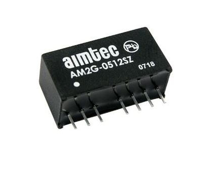 12V DC-DC Converter AM2G-0512SZ: Specifications, Datasheet, Applications and Features6/3/2024 517
A DC-DC converter is an essential electronic device to convert a direct current (DC) source from one voltage level to another. These converters are widely employed in various applications, including portable electronic devices, automotive systems, and renewable energy installations.
Read More >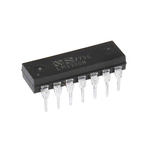 What is LM3900 Quadruple Norton Operational Amplifier?5/30/2024 1103
The LM3900 consists of four independent dual-input internally compensated amplifiers. These amplifiers are specifically designed to operate on a single power supply voltage and provide a large output voltage swing. They utilize current mirrors to achieve in-phase input functionality. Applications include AC amplifiers, RC active filters, low-frequency triangle waves, square wave, and pulse waveform generation circuits, tachometers, and low-speed, high-voltage digital logic gates.
Read More > Exploring the MMBT3906 Transistor: A Comprehensive Guide5/24/2024 738
The goal of the Taiwan Semiconductor MMBT3906 PNP Bipolar Transistor is to provide a high surge current capability with minimal power loss. This transistor is perfect for automated installation and has high efficiency.
Read More >
SUPPORT
ABOUT BITFOIC
QUICK LINKS
Connect with us
Tel: 86-755-23606554
E-mail: [email protected]
Address: Room A29, 24 / F, Hoi Tak Wai, Prince Edward industrial building, 706 Prince Edward Road East, San Po Kong, Kowloon,Hongkong
Mon-Fri: 09.30 AM - 18.30 PM


